Home » Solar Energy » What is Solar Energy?
What is Solar Energy?
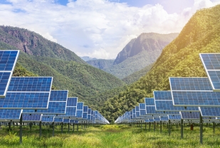
Solar energy refers to the thermal radiation energy of the sun, which uses sunlight to convert energy into usable forms, such as electricity and heat. In a broad sense, solar energy also includes wind energy, chemical energy, water energy, etc. Solar energy is a clean and renewable energy source. Since the birth of life on Earth, it has mainly relied on the thermal radiation energy provided by the sun to survive. Especially now that fossil fuels are dwindling, solar energy has become an important source of energy for human beings, and continues to develop. The utilization of solar energy is mainly through two methods: photothermal conversion and photoelectric conversion. Solar power generation is an emerging renewable energy source.
The Sun's Energy
Solar energy is a primary energy source. Primary energy refers to energy obtained directly from nature and can be divided into two categories. The first group includes those energy sources that will be exhausted by exploiting them. These energy sources are called the depleting energy sources and they are the fossil fuels and nuclear energy. The fossil fuels and nuclear power are the main source of energy in today’s energy system and they supply 78% of the energy demand. Under the assumption that the population of mankind does not change drastically and it consumes energy at the current level, the fossil fuel reserves will be exhausted within 320 years and the nuclear energy within 260 years. This can seem a very long time for us. However, when we compare this period the time span of existence of the Earth or the human civilization, it is a negligible fraction of time. We have to be aware that the reserves of fossil fuels on the Earth are limited and will be exhausted.

Solar energy is energy released through nuclear fusion reactions inside the sun. The surface temperature reaches 5800 Kelvin. It will last another 5 billion years, and this energy can be directly utilized by humans.
The average amount of the sun's radiation that penetrates the atmosphere and reaches the Earth is 51% of the total incoming energy. Of the 49% that does not reach the Earth, 30% is reflected back into space and 19% is absorbed by the atmosphere and clouds. The total solar energy absorbed by Earth's atmosphere, oceans, and land masses is approximately 3,850,000 exajoules (EJ) per year. The earth's energy use by mankind is approximately 500 exajoules per year. This is about 0.01% of the total yearly energy coming from the sun. Putting this in another way, the earth absorbs more energy in one hour than the world uses in one year according to physicist Steven Chu, US Energy Secretary and former Director of Lawrence Berkeley National Laboratory. In total, the sun emits about 2.2 billion times the amount of radiation that is received by the earth. If this solar energy can be collected through solar cells, it will be of great significance to the sustainable development of the Earth.
World Solar Radiation Map

The map above shows in maroon, red, and orange the prime regions of the world for generating solar electricity. There are enough strong solar regions to one day provide all the energy that is needed by mankind.
Solar Radiation Spectrum
 Shown in the diagram is how the energy from the sun is distributed by wavelength and photon energy. As one can see, a good portion of the sun's radiation is in the visible range (46%). Radiation in the ultraviolet region (5%), which is not visible, causes the skin to tan and has more energy than that in the visible region. Radiation in the infrared region (49%), which we feel as heat, has slightly more total energy than the radiation in the visible region.
The shape of the spectrum is almost a perfect fit for a heavenly body whose temperature is 5,800 Kelvin. This is how we know with good accuracy the temperature at the sun's surface.
Other stars have enormous sources of energy in the form of high-energy X-rays, but lucky for us, our sun releases almost half of its energy as visible light.
Solar Insolation
What is the difference between radiance and insolation? For ordinary people, they are probably the same thing. To a scientist, there is a distinct difference. Radiation is usually short for electromagnetic radiation and radiance is an instantaneous measurement at a distinct point in time. Solar radiation “emits” from the sun equally in all directions at frequencies that are visible and non-visible. On the other hand “insolation” is the amount of radiation “received” on a given surface (usually a square meter) on a plane perpendicular to the sun in a given amount of time (usually a day). The name comes from a combination of the words “incident solar radiation”.
 Over the course of a year, the average solar “radiance” arriving at the top of the earth's atmosphere is 1,367 watts per square meter-called the “solar constant”. The solar constant varies by up to ±3% per day as the Earth orbits the sun. Because of losses in the atmosphere (about 50%), different angles to the sun from the equator to the poles (averages 50%), and no sunlight during nighttime (another 50%), the average “daily insolation” for the average position on earth (ignoring clouds) is about 170 watts per square meter (one-eigth the solar constant). However, insolation varies quite a bit from place to place. Typical values are about 200 W/m2 in Australia, 185 W/m2 in the United States, and 105 W/m2 in the United Kingdom. Shown in the figure above is the insolation by time of day and month of the year for Cairo, Egypt. Cairo has approximately the same latitude and weather pattern as Phoenix, Arizona. It demonstrates how an "average" daily insolation can be misleading considering winter and summer extremes.
The Sun's Energy
Solar energy is a primary energy source. Primary energy refers to energy obtained directly from nature and can be divided into two categories. The first group includes those energy sources that will be exhausted by exploiting them. These energy sources are called the depleting energy sources and they are the fossil fuels and nuclear energy. The fossil fuels and nuclear power are the main source of energy in today’s energy system and they supply 78% of the energy demand. Under the assumption that the population of mankind does not change drastically and it consumes energy at the current level, the fossil fuel reserves will be exhausted within 320 years and the nuclear energy within 260 years. This can seem a very long time for us. However, when we compare this period the time span of existence of the Earth or the human civilization, it is a negligible fraction of time. We have to be aware that the reserves of fossil fuels on the Earth are limited and will be exhausted.
The average amount of the sun's radiation that penetrates the atmosphere and reaches the Earth is 51% of the total incoming energy. Of the 49% that does not reach the Earth, 30% is reflected back into space and 19% is absorbed by the atmosphere and clouds. The total solar energy absorbed by Earth's atmosphere, oceans, and land masses is approximately 3,850,000 exajoules (EJ) per year. The earth's energy use by mankind is approximately 500 exajoules per year. This is about 0.01% of the total yearly energy coming from the sun. Putting this in another way, the earth absorbs more energy in one hour than the world uses in one year according to physicist Steven Chu, US Energy Secretary and former Director of Lawrence Berkeley National Laboratory. In total, the sun emits about 2.2 billion times the amount of radiation that is received by the earth. If this solar energy can be collected through solar cells, it will be of great significance to the sustainable development of the Earth.
World Solar Radiation Map
Solar Radiation Spectrum
The shape of the spectrum is almost a perfect fit for a heavenly body whose temperature is 5,800 Kelvin. This is how we know with good accuracy the temperature at the sun's surface.
Other stars have enormous sources of energy in the form of high-energy X-rays, but lucky for us, our sun releases almost half of its energy as visible light.
Solar Insolation
What is the difference between radiance and insolation? For ordinary people, they are probably the same thing. To a scientist, there is a distinct difference. Radiation is usually short for electromagnetic radiation and radiance is an instantaneous measurement at a distinct point in time. Solar radiation “emits” from the sun equally in all directions at frequencies that are visible and non-visible. On the other hand “insolation” is the amount of radiation “received” on a given surface (usually a square meter) on a plane perpendicular to the sun in a given amount of time (usually a day). The name comes from a combination of the words “incident solar radiation”.
Post a Comment:
You may also like:
Category
Featured Articles
Expanding Research on Solar Energy ...
The application fields of solar energy are very wide, covering many fields such as the photonic industry, new energy photothermal ...
Exploring Concentrated Solar Power ...
Concentrated Solar Power (CSP) systems use very different technology than photovoltaic systems. CSP systems use the sun as the ...
Solar Cell Manufacturing Process
Solar cells are made of various materials, the most common of which include silicon, indium gallium, cadmium selenide, etc. These ...
The Evolution of Grid Electricity ...
"Electricity" cannot be stored on the grid; generation must be approximately equal to consumption at all times. However, ...
Solar Activity: Sunspots, Magnetism & ...
Solar activity refers to a series of complex phenomena in the solar atmosphere, including sunspots, flares, prominences, coronal ...